nanophotonics.ca
Nanophotonics nanoelectronics: Home
The nanophotonics group of Professor Andreas Ruediger. At INRS-EMT, Université du Québec. Is dedicated to nanoscale oxide electronics, their physical properties and applications. Our investigations are based on advanced scanning probe techniques in combination with optical spectroscopy. Funded by the Canadian Foundation of Innovation provides an internationally competitive infrastructure operated by an interdisciplinary team.
 nanophotonics.com.au
Index of /
Research and Consultancy: Optics, Acoustics, Environment. Nanophotonics, Plasmonics and Nano-Optics: Consultancy, Research. Nano-optics investigates optical waves localized beyond the diffraction limit of light into nano-scale regions with dimensions as small as a few nanometers (i.e., much smaller than the wavelength). What Do We Do? Consultancy, research, theoretical and numerical modelling in nanophotonics, plasmonics and nano-optics for government and private organisations in the following areas:.
 nanophotonics.csic.es
García de Abajo's Nanophotonics Theory Group at ICFO
We are currently offering PhD and postdoc positions in our group. Contact ICREA Prof. F. Javier García de Abajo (javier.garciadeabajo@icfo.es and 34-653700342) for more information. PEOPLE - Group members. PUBLICATIONS - Full access to our published works. WIDGETS - Self-contained online simulations of specific phenomena related to our research. GALLERY - Journal covers from our work.
 nanophotonics.de
nanophotonics.de
The Sponsored Listings displayed above are served automatically by a third party. Neither the service provider nor the domain owner maintain any relationship with the advertisers. In case of trademark issues please contact the domain owner directly (contact information can be found in whois).
 nanophotonics.ece.cornell.edu
Cornell Nanophotonics Group - School of Electrical and Computer Engineering - Cornell Engineering
Skip to main content. School of Electrical and Computer Engineering. Cornell Nanophotonics Group Moved to Columbia. Broadband mid-infrared frequency comb generation in a Si3N4 microresonator. Kevin Luke, Yoshitomo Okawachi, Michael R. E. Lamont, Alexander L. Gaeta, Michal Lipson, Optics Letters, Vol. 40, No. 21, 19 Oct. 2015. Synchronization and Phase Noise Reduction in Micromechanical Oscillator Arrays Coupled through Light. Optical nonlinearities in high-confinement silicon carbide waveguides. Prof Lip...
 nanophotonics.eecs.berkeley.edu
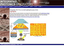
IPL: Integrated Photonics Laboratory
20 September 2012: We are currently updating the group website. Ming Wu's group has recently developed a new image-driven optical manipulation tool called optoelectronic tweezers. Using light-induced dielectrophoresis on a photoconductor, virtual electrode pattern is generated by projecting an LED light through a DMD spatial light modulator. A single LED is capable of generating more than 15,000 individually addressable traps. The results was published in the July 21, 2005 issue of Nature titled,.
 nanophotonics.etu.edu.tr
Kurt Research Group – Nanophotonics Lab
Slow light in photonic structures. Efficient Light Detection in Photonic Structures. Optical Cloaking and Invisibility. Inverse Design for Nanophotonics. ELE 452 552 Photonics. ELE 453-553 Optical Communication. Our group is led by Professor Hamza Kurt. Specific topics of interests include:. Slow light in photonic structures. Optical cloaking and invisibility. Inverse design of nanophotonic structures. Efficient light detection in photonic structures. Novel photonic crystal device designs.
 nanophotonics.gatech.edu
Georgia Institute of Technology :: Nanophotonics Research Group
Georgia Institute of Technology. Materials Science and Engineering. Georgia Tech Research Institute. Phosphor Technology Center of Excellence. Defense Advanced Research Projects Agency (DARPA). Advanced Technology Development Center. The Society for Information Display. The International Society for Optical Engineering. The Optical Society of America. Several of our publications were selected for the Virtual Journal of Nanoscale Science and Technology. Appl Phys. Lett. ZnS:Mn multilayer inverse opals.
 nanophotonics.hnu.cn
湖南大学
湖南大学版权所有 1996,2000,2010,2017年 通讯地址:湖南省长沙市岳麓区麓山南路麓山门 邮编 410082 Email xiaoban@hnu.edu.cn. 域名备案信息 [www.hnu.edu.cn,www.hnu.cn/湘ICP备09007699号] [hnu.cn 湘教QS3-200503-000481 hnu.edu.cn 湘教QS4-201312-010059].
 nanophotonics.iitd.ac.in
Home-Nanophotonics, Nanophotonics Lab IIT Delhi, Nanophotonics IIT Delhi, Indian Institute of Technololgy Delhi, Nano Lab, photonics IIT Delhi, Nano research in iit delhi, Photonics in iit delhi, Nanophotonics in iit delhi, research in nanophotoics, iit de
The new emerging paradigm where light interacts with nano-scaled structures and brings forth the mysterious world to research.The combination of Photonics and Nanotechnology giving birth to Nanophotonics compliments and benefits each other in terms of new functions, materials, fabrication processes and applications. Nanophotonic research activity has been initiated in IIT Delhi in 2005. Recently IIT Delhi has recognized our research as one of the High-impact research activity.
 nanophotonics.info
RINPS NPOナノフォトニクス工学推進機構
ドレストフォトン表面平坦化装置 のパンフレットをアップロード致しました [ PDF 1.3MB. ドレストフォトン表面修復装置 のパンフレットをアップロード致しました [ PDF 1.3MB. ドレストフォトン微細加工装置 DPF-100 のパンフレットをアップロード致しました [ PDF 5.4MB. エディターズ ノート にて 発光するSi、今度は本物か. 4月号にて SiやSiCが様々な色で発光 ドレスト光子 で実現. 大日本印刷(株)ニュースリリース 4月2日 にて、 横浜国立大学、情報通信研究機構、東京大学と共同でナノレベルのランダムパターンで個体認証する技術 ナノ人工物メトリクス を開発. 日本経済新聞 4月2日、16面 にて、 偽造防ぐナノ刻印 ICカードなど対象 と題する記事が掲載されました。 11月25日、 なるほどランド にて、 粘菌でコンピューター進化. 日本経済新聞 10月2日、14面 にて、 次世代半導体 粘菌がお手本 と題する記事が掲載されました。 大津元一 成瀬誠 八井崇 著、朝倉書店 2009. 大津元一 斎木敏治 戸田泰則 著、朝倉書店 2009.